Wafer Scale Manufacturing
The Tru-SiPh™ platform was built from the ground up to disrupt the traditional photonics markets in multiple applications. Tru-SiPh™ is being designed into ethernet pluggable modules, into copackaged optics, into Lidar, and into biosensor applications. Using our own high volume silicon foundry, we have developed a proprietary process for embedding III-V compounds within our silicon wafers, providing a high-performance wafer scale platform with all the advantages of traditional InP based optics, but without the discrete construction and alignments which are typically used. Our proprietary technology provides unique temperature insensitive optics allowing uncooled use in most applications.
Architecture
With embedded lasers, modulators and photodiodes, the architecture is extremely compact compared to other approaches and contains all necessary elements for any optical function. Resulting products are natively hermetically sealed and require no additional packaging. By bonding thin eitaxies directly to the silicon substrate, our structures outperform traditional InP based optics for thermal performance resulting in very compact long-lived active elements. Serving all applications in O- and C- band, with a variety of components (see toolbox below), the platform was designed from the ground up to be application agnostic.
Optical Toolbox
What is in our tool box of Tru-SiPh™ components?
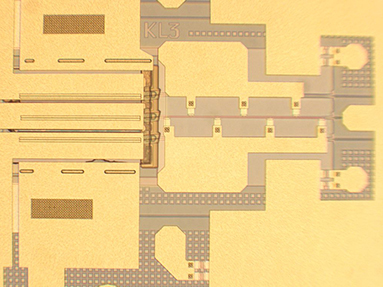
Lasers
-
Single frequency long cavity external DBR lasers in C- and O-bands
-
Full C-band or O-band tunable lasers with narrow linewidth <70kHz)
controllable to <10pm
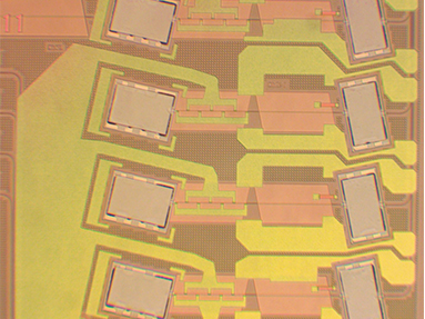
Modulators
-
Electroabsorbtion modulators with <1.5V
p-p drive voltage -
InP based Mach Zender modulators with a fraction the size of silicon MZ modulators
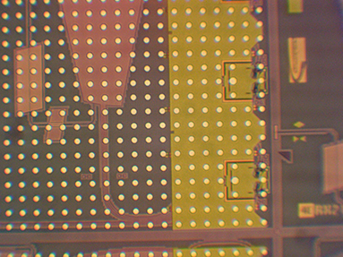
Photodiodes
-
High bandwidth, high efficiency
end-coupled photodiodes -
Short cavity monitor photodiodes
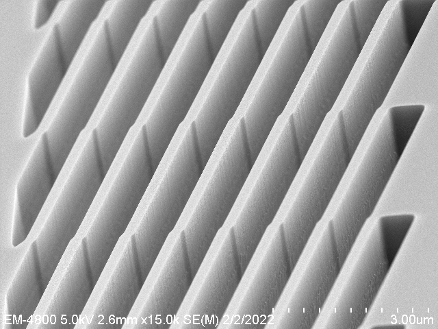
Optical elements
-
Tuning free mux and demux for O- and C- band
-
Gratings
-
Couplers and splitters
-
Polarization control elements, splitters
-
Low loss waveguides with 5um bend radii
Light coupling
-
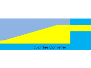
Spot size converters for simplified coupling to fiber
-
Optical phased array for free space transmission
Latest News
Skorpios Tru-SiPh Achieves Record 0.35 FIT Laser Reliability, Setting New Benchmark for Silicon Photonics Infrastructure
Skorpios Technologies, Inc., a leader in heterogeneous silicon photonics and advanced semiconductor manufacturing, today released a technical…
Skorpios Unveils Revolutionary 1.6 Tbps and 6.4 Tbps Optical Engines to Deliver Lowest Cost-per-Bit for AI Data Centers
Skorpios Technologies, a leader in heterogeneous silicon photonics and advanced semiconductor manufacturing, today announced its breakthrough Tru-SiPh™…
