Our Fab
Our devices are fabricated in highly proprietary processes in our Austin Texas silicon microstructures foundry. This fab has a 40 year history of providing unique solutions to the silicon and CMOS industry and continues to do so to this day. Using CMOS process tools and unique processes, the Tru-SiPh™ platform is fabricated, tested, and burned-in with a wafer scale process that radically changes the economics of high-performance optics. Our fab also supports integration structures for 2.5D and 3D packaging, useful for higher level integration and copackaged optics. In addition, Skorpios has its own high-volume tools for production of III-V epitaxy. Growth chambers are able to support up to 3x200mm wafers in one growth.
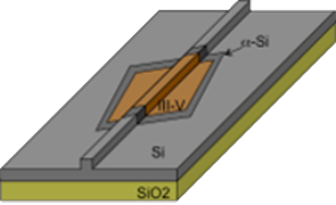
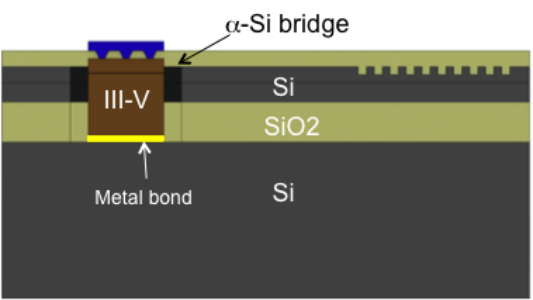
The tight waveguide confinement and embedded epitaxies allow for very high levels of integration in compact form factors for high yield and low cost. The architecture allows each epitaxy to be used for multiple purposes, without additional cost. For instance, redundant lasers are simply implemented with lithography on an existing epitaxy.

The tight waveguide confinement and embedded epitaxies allow for very high levels of integration in compact form factors for high yield and low cost. The architecture allows each epitaxy to be used for multiple purposes, without additional cost. For instance, redundant lasers are simply implemented with lithography on an existing epitaxy.

The tight waveguide confinement and embedded epitaxies allow for very high levels of integration in compact form factors for high yield and low cost. The architecture allows each epitaxy to be used for multiple purposes, without additional cost. For instance, redundant lasers are simply implemented with lithography on an existing epitaxy.

The tight waveguide confinement and embedded epitaxies allow for very high levels of integration in compact form factors for high yield and low cost. The architecture allows each epitaxy to be used for multiple purposes, without additional cost. For instance, redundant lasers are simply implemented with lithography on an existing epitaxy.
With embedded lasers, modulators and photodiodes, the architecture is extremely compact compared to other approaches and contains all necessary elements for any optical function. Resulting products are natively hermetically sealed and require no additional packaging. By bonding thin eitaxies directly to the silicon substrate, our structures outperform traditional InP based optics for thermal performance resulting in very compact long-lived active elements. Serving all applications in O- and C- band, with a variety of components (see toolbox below), the platform was designed from the ground up to be application agnostic.
Wafer Bonding
Lorem ipsum dolor sit amet, consectetur adipiscing elit. Sed eget consequat elit. Proin dignissim efficitur nisl eget dictum. Mauris congue sit amet orci vel lobortis. Fusce consequat sem libero.
Wafer Bonding
Lorem ipsum dolor sit amet, consectetur adipiscing elit. Sed eget consequat elit. Proin dignissim efficitur nisl eget dictum. Mauris congue sit amet orci vel lobortis. Fusce consequat sem libero.
Wafer Bonding
Lorem ipsum dolor sit amet, consectetur adipiscing elit. Sed eget consequat elit. Proin dignissim efficitur nisl eget dictum. Mauris congue sit amet orci vel lobortis. Fusce consequat sem libero.
Overview
Lorem ipsum dolor sit amet, consectetur adipiscing elit. Sed eget consequat elit. Proin dignissim efficitur nisl eget dictum. Mauris congue sit amet orci vel lobortis. Fusce consequat sem libero, a pellentesque neque blandit vitae. Duis ut turpis aliquam, iaculis mauris id, vulputate nisi. Curabitur accumsan, enim eu finibus pulvinar, lacus arcu varius orci, vitae consectetur libero ipsum nec dolor. Aenean eget velit vel nisl dictum sollicitudin. Phasellus rhoncus diam ac tortor pretium, et faucibus ante fermentum. Phasellus vel ligula eu diam fringilla porttitor. Aliquam eu eros magna. Donec at varius ligula. Nulla vestibulum tortor nunc, vitae varius ex lacinia vel. Duis eget elit vitae ipsum dictum rhoncus. Vestibulum vel bibendum felis, vitae tristique orci. Morbi sed tempor tortor. Nulla feugiat eros ut efficitur egestas.

The tight waveguide confinement and embedded epitaxies allow for very high levels of integration in compact form factors for high yield and low cost. The architecture allows each epitaxy to be used for multiple purposes, without additional cost. For instance, redundant lasers are simply implemented with lithography on an existing epitaxy.